
I2C Basics:
Note:
This guide is purposefully simple and does not address some of the more intricate details of I2C (for now). For more information on I2C, please refer to the following: NXP UM10204 I2C-bus specification and user manual.
Another thing worth noting is that traditionally, electrical engineers used “master/slave” to refer to I2C devices and these terms are often found in reference materials. To avoid confusion when reading, please note that this document is aligned with the latest I2C specification (I2C v.7) which updated these terms to be “controller/target”.
What is I2C?
- Originally created in 1982 by Philips (now NXP semiconductor) as a simple 2-wire serial bus.
- Uses only one data and one clock line to allow a single controller to interface with multiple targets.
- I2C is very popular because it requires a lower amount of gates to implement compared to other similar protocols and only requires two pins. Both of which reduce cost.
- I2C is half duplex.
Protocol Details:
- The controller initializes communication and provides the clock signal (the SCL line is used to share the clock signal).
- I2C supports Controller-Target communication. Only two devices may use the bus at any given time.
- The clock signal effectively sets the data transfer rate for the
system.
- There is a maximum clock frequency for a given I2C mode but no minimum clock speed.
- The data line (SDA) is bidirectional which means that the controller can read and write to/from targets.
- Since I2C is a serial bus, data is transmitted one bit at a time in sync with the clock rate.
- Multiple controllers may share a bus. (Note: the full I2C specification covers arbitration and clock synchronization for this case.)
- Each device on the bus has a unique address, there are some reserved
addresses for certain features.
- Without the use of multiplexers, every device on the bus must have a unique address to prevent crowding.
- The target can either be recieve only or act as an I2C transceiver.
- I2C hardware designs must account for capacitive loading on the bus
from parasitic capacitance of the signal lines and input capacitance of
devices on the bus.
- It is recommended to not exceed 400pF of capacitive loading to keep rise times in an acceptable range.
I2C Communication Modes:
| I2C Mode: | Speed (<=) | Bus Direction |
|---|---|---|
| Standard Mode (SM) | 100 Kbps | Bidirectional |
| Fast Mode (FM) | 400 Kbps | Bidirectional |
| Fast Mode Plus (FM+) | 1 Mbps | Bidirectional |
| High Speed Mode (HS-Mode) | 3.4 Mbps | Bidirectional |
| Ultra-Fast Mode (UFM) | 5 Mbps | Unidirectional |
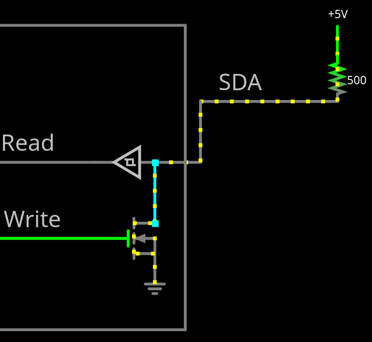
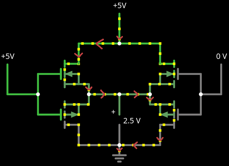
Circuit Description:
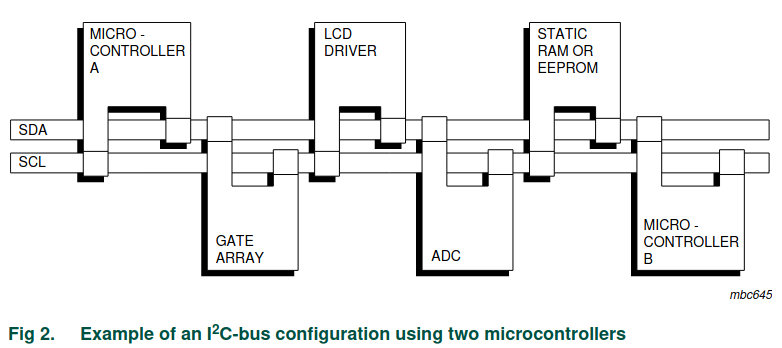
Pullup resistors pull SDA and SCL up to VDD. This is required for I2C since the protocol is designed to have open drain (CMOS) or open collector (BJT) devices on the bus. This way each device can easily pull the line low with one transistor instead of using two in a push pull configuration. Another benefit of this configuration is that the bus cannot be crowded by two devices trying to pull a line to opposite logic levels. This can result in indeterminate behavior and high currents flowing from high to low potential (see diagram).
Basic I2C Communication Frame Structure:
- The controller must wait until the bus is free.
- SDA and SCL must both be high for the bus to be free.
- The controller then pulls the SDA line low while keeping SCL in the
default state (high, no clocking).
- This is known as the start condition and triggers all other devices on the bus to listen for their address to be called in the next step.
- The controller starts providing the clock signal on SCL. All other
devices on the bus will use this signal as a reference for when logic
level changes on the SDA line are valid.
- Apart from the start and stop conditions, no device on the bus may change the state of SDA unless SCL is pulled low.
- The controller now sends a 7-bit address field.
- 10-bit addressing format:
- 10-bit addressing works by sending
0b1110XXas the 7-bit address (whereXXare the two MSBs of the 10-bit address), a read/!write bit (see next list entry), an acknowledge bit field to see if there are any 10-bit devices on the bus, finally followed by the 8 remaining bits of the address and a second acknowledge field for the device at the specified 10-bit address.
- 10-bit addressing works by sending
- 10-bit addressing format:
- The controller will then send the Read/!Write bit to signify whether
the next operation will be a read request or a write operation.
- Read is active high, write is active low.
- At this stage, the device that was addressed earlier (the target) is
expected to acknowledge so the controller knows it’s on the bus and
ready to communicate.
- To acknowledge, the target will pull SDA low. This is known as an “ACK bit”.
- If no device acknowledges the bus will continue to be pulled high by the pullup resistors since the controller released the line. This is known as an “NACK bit” (No Acknowledge).
- NOTE: All ACK/NACK signals must be sent by a receiver.
- If the receiver sent an ACK the data transfer process may follow.
- Otherwise the operation is canceled.
- Data transfer is done in an unlimited sequence of 8-bit words.
- After every 8-bit frame, the receiving device is expected to send an ACK signal to ensure synchronization and that data is still making it to the receiving device.
- It is standard procedure for most devices to cancel data transmission if an NACK is sent at this stage but the specification allows for other scenarios. The datasheet of a device should be consulted to determine its behavior since a NACK signal may also represent other things (access delay, an interrupt is being serviced, etc).
- Some devices use a repeated start condition and will repeat the control byte to signify continued data transfer.
- When the data transfer is finished, the controller transitions SDA from low to high while holding SCL high. This is called the stop condition and tells other devices that the bus is now free.
In a system with multiple controllers, a controller may use a general call to identify themselves to other devices on the bus (See Reserved Addresses and section 3.1.13 of the I2C spec NXP UM10204).
Anatomy of an I2C Waveform:
Example I2C frame with two bytes of data transfer:
             S
             T                                                                                                           N   S
             A                               R   A                                   A                                   A   T
             R                               /   C                                   C                                   C   O
     FREE    T       A5  A4  A3  A2  A1  A0  !W  K   D7  D6  D5  D4  D3  D2  D1  D0  K   D7  D6  D5  D4  D3  D2  D1  D0  K   P   FREE
     ______      __  __  __  __  __  __  __  __      __  __  __  __  __  __  __  __      __  __  __  __  __  __  __  __  __      ____...
SDA:       \    /  \/  \/  \/  \/  \/  \/  \/  \    /  \/  \/  \/  \/  \/  \/  \/  \    /  \/  \/  \/  \/  \/  \/  \/  \/  \    /
            \__/\__/\__/\__/\__/\__/\__/\__/\__/\__/\__/\__/\__/\__/\__/\__/\__/\__/\__/\__/\__/\__/\__/\__/\__/\__/\__/    \__/

                 X   X   X   X   X   X   X   X   0   X   X   X   X   X   X   X   X   0   X   X   X   X   X   X   X   X   1

SCL: ──────────┐ ┌─┐ ┌─┐ ┌─┐ ┌─┐ ┌─┐ ┌─┐ ┌─┐ ┌─┐ ┌─┐ ┌─┐ ┌─┐ ┌─┐ ┌─┐ ┌─┐ ┌─┐ ┌─┐ ┌─┐ ┌─┐ ┌─┐ ┌─┐ ┌─┐ ┌─┐ ┌─┐ ┌─┐ ┌─┐ ┌─┐ ┌─┐ ┌───────...
               └─┘ └─┘ └─┘ └─┘ └─┘ └─┘ └─┘ └─┘ └─┘ └─┘ └─┘ └─┘ └─┘ └─┘ └─┘ └─┘ └─┘ └─┘ └─┘ └─┘ └─┘ └─┘ └─┘ └─┘ └─┘ └─┘ └─┘ └─┘
Reserved-Addresses:
I2C device addresses must not conflict with reserved addresses.
| Target address | R/!W bit | Description |
|---|---|---|
| 0000 000 | 0 | General call |
| 0000 000 | 1 | START byte |
| 0000 001 | X | CBUS address |
| 0000 010 | X | Reserved for different bus formats on a shared bus |
| 0000 011 | X | Reserved for future purposes |
| 0000 1XX | X | Hs-mode controller code |
| 1111 1XX | 1 | Device ID |
| 1111 0XX | X | 10-bit target addressing |
End!
There are still some concepts in I2C that still need to be covered and will probably be added later. In the interim if you need more details, the I2C specification is the most accurate source of information. Hopefully this overview helped you in some form or another!!